Description
Analog-to-digital conversion (ADC) is necessary because, while embedded systems deal with digital values, their surroundings typically involve many analog signals such as, temperature, speed, pressure, the output of a microphone, etc. They all need to be converted into digital data before being processed by the microcontroller. Today, we will see how to read an external analog signal using a PIC16F688 microcontroller, and display the conversion output (a digital number) on a LCD. The input analog signal will be a varying voltage between 0-5V derived using a potentiometer.
Required Theory
The PIC16F688 microcontroller has a built-in 10-bit ADC with eight input channels. The eight channels are available at RA0, RA1, RA2, RA4, RC0, RC1, RC2, and RC3. They have alternate labels, AN0-AN7, for this function, and are multiplexed into a single Sample and Hold circuit. The output of the Sample and Hold is connected to the input of the A/D converter. The 10-bit conversion result is stored into the ADC result registers ADRESH (A/D Result Higher byte) and ADRESL (A/D Result Lower byte). Each of these registers is 8-bit. The functionality of the A/D module is controlled by three registers: ANSEL, ADCON0, and ADCON1. The details of these control registers are discussed in ADC channels in PIC16F688.
Circuit Diagram
The test circuit to demonstrate the 10-bit A/D conversion using PIC16F688 is shown below. The test input voltage for ADC is derived from a 5K potentiometer connected across the +5V power supply, and is connected to RA2/AN2 pin of PIC16F688. The supply voltage (+5V) is chosen as the reference voltage for A/D conversion. Therefore, the 10-bit ADC will convert any analog voltage between 0-5V to a digital number ranging from 0-1023. The number will be displayed on the LCD.
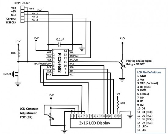
Circuit diagram
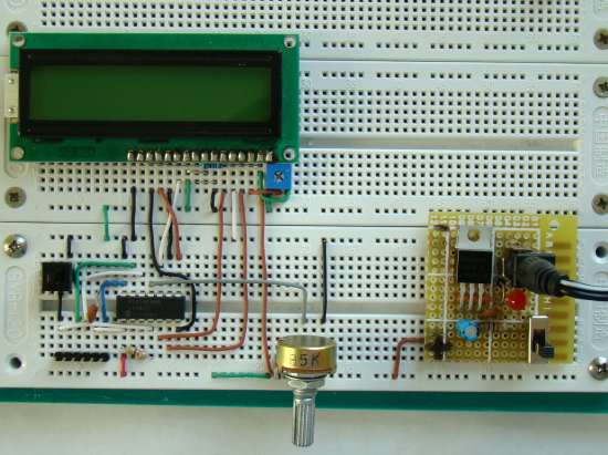
Circuit setup on breadboard
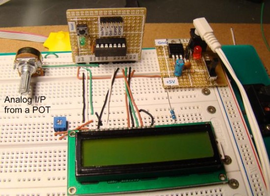
Circuit setup using the PIC16F688 breadboard module
The programming involves configuring ANSEL, ADCON0, and ADCON1 registers. Since RA2/AN2 is used as analog input, the corresponding ANSEL bit must be set. In ADCON0 register, set CHS1 and clear CHS0 and CHS2, so that the AN2 channel will be connected to the internal Sample and Hold circuit. Clearing the VCFG bit in ADCON0 will select the supply voltage (+5V) as the reference voltage for A/D conversion. The ADCON1 register is used to select the clock source for A/D conversion. However, the MikroC Pro for PIC has got a built-in library function named ADC_Read() that, by default, uses the internal RC clock for ADC operation. So you don’t need to initialize the ADCON1 register. The complete program is given below.
/* Lab 5: Analog-to-digital converter Internal Oscillator @ 4MHz, MCLR Enabled, PWRT Enabled, WDT OFF Copyright @ Rajendra Bhatt October 10, 2010*/// LCD module connections sbit LCD_RS at RC4_bit; sbit LCD_EN at RC5_bit; sbit LCD_D4 at RC0_bit; sbit LCD_D5 at RC1_bit; sbit LCD_D6 at RC2_bit; sbit LCD_D7 at RC3_bit; sbit LCD_RS_Direction at TRISC4_bit; sbit LCD_EN_Direction at TRISC5_bit; sbit LCD_D4_Direction at TRISC0_bit; sbit LCD_D5_Direction at TRISC1_bit; sbit LCD_D6_Direction at TRISC2_bit; sbit LCD_D7_Direction at TRISC3_bit;// End LCD module connections// Define Messages char message1[] = "ADC Value= "; char *temp = "0000"; unsigned int ADC_Value; void main() { ANSEL = 0b00000100; // RA2/AN2 is analog input ADCON0 = 0b00001000; // Analog channel select @ AN2 CMCON0 = 0x07 ; // Disbale comparators TRISC = 0b00000000; // PORTC All Outputs TRISA = 0b00001100; // PORTA All Outputs, Except RA3 and RA2 Lcd_Init(); // Initialize LCD Lcd_Cmd(_LCD_CLEAR); // CLEAR display Lcd_Cmd(_LCD_CURSOR_OFF); // Cursor off Lcd_Out(1,1,message1); // Write message1 in 1st row do { adc_value = ADC_Read(2); temp[0] = adc_value/1000 + 48; // Add 48 to get the ASCII character value temp[1] = (adc_value/100)%10 + 48; temp[2] = (adc_value/10)%10 + 48; temp[3] = adc_value%10 + 48; Lcd_Out(1,11,temp); Delay_ms(2000); } while(1); }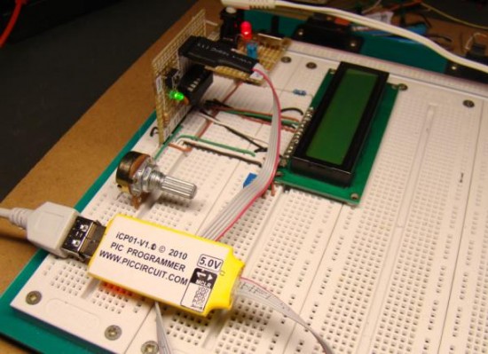
Loading the HEX file with my handy iCP01 PIC programmer.
Output
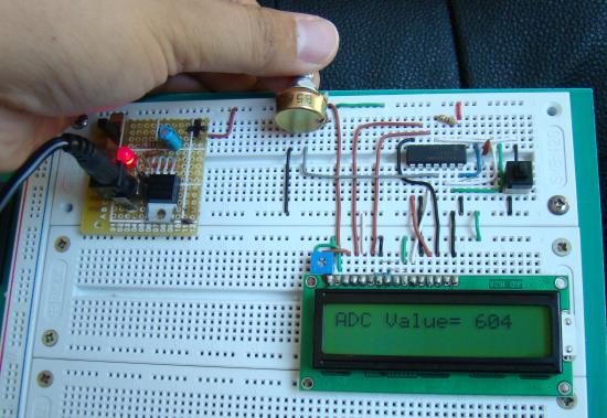
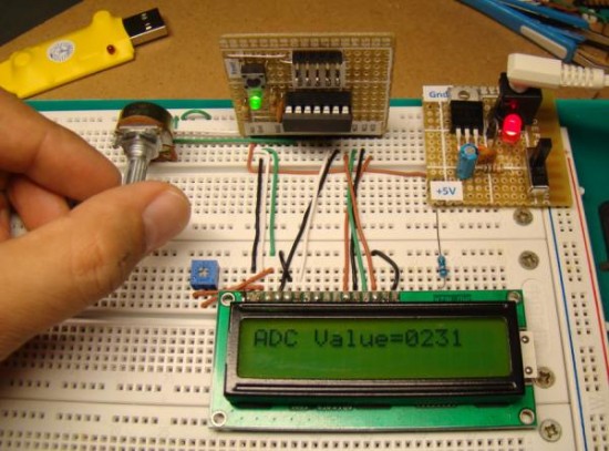
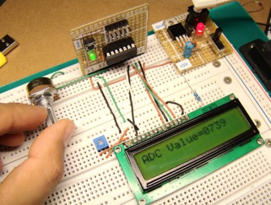
Vary the potentiometer and you will see the 10-bit conversion result also vary proportionally from 0- 1023.

 Posted in:

0 comments:
Post a Comment